Features Title Here. Consectetur adipisicing

Features Content Here. Sit amet, consectetur adipisicing elit, sed do eiusmod tempor incididunt ut labore et dolore magna aliqua. Ut enim ad minim veniam, quis nostrud exercitation ullamco laboris nisi ut aliquip ex ea commodo consequat.

Differentiator

Tuesday, July 12, 2011

Introduction :

An operational amplifier is a direct-coupled high amplifier usually consisting of one or more differential amplifiers and usually followed by a level translator and an output stage. The output stage is generally a push-pull complementary-symmetry pair. An operational amplifier is available as a single integrated circuit package.

The operational amplifier is a versatile device that can be used to amplify dc as well as ac input signals and was originally designed for performing mathematically operations such as addition, subtraction, multiplication and integration

A differentiator is obtained by interchanging the resistor and the capacitor of an integrator. The output voltage is the negative of the derivative of the input signal. The differentiator or differentiation amplifier is the circuit performs the mathematical operation of differentiation; that is the output waveform is the derivative of the input waveform.

 Description:

Circuit Diagram:  


Fig 2(a): Basic differentiator

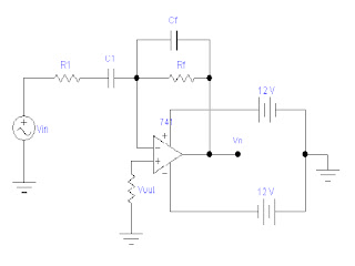
Fig 2(b): Practical differentiator circuit

 
Operation principal: The differentiator may be constructed from a basic inverting amplifier if an input resistor R1 is place by a capacitor C1.

The expression for the output voltage can be obtained from Kirchoff current Law equation written at node v2 as follows:  
 
         ic = IB + iF
 Since IB    0                        ic = iF                            


Thus the output Vo is equal to RFC1 times the negative instantaneous rate of change of the input voltage  Vin
 with time. Since the differentiator performs the reverse of the integrators function, a cosine wave input will produce a sine output, or a triangular input will produce a square wave output.

The gain of the circuit increases with increase in frequency at a rate of 20 dB /decade. This makes the circuit unstable. Also, the input impedance XC1 decreases with increase in frequency, which makes the circuit very susceptible to high-frequency noise. When amplified, this noise can completely override the differentiated output signal. The frequency response of the basic differentiator is shown in Fig 3. In this figure, fa is the frequency at which the gain is o dB and is given by

 Also, fc is the unity gain-bandwidth of the op-amp and f is some relative operating frequency. Both the 
stability and the high-frequency noise problems can be corrected by the addition of two components: R1 and CF, as shown in Fig 2(b). This circuit is a practical differentiator, the frequency response of which is shown in Fig 3 by a dashed line. From frequency f to fb the gain increases at 20 dB/decade. However, after fb the gain decreases at 20 dB/decade. This 40 dB/decade change in gain is caused by the R1C1 and RFCF combinations. The gain limiting frequency fb is given by


I.        Conclusion
Advantage:
1.   The differentiator is most commonly used in wave shaping circuit to detect high frequency components in an input signal. 
2.    It is a rate-of-change detector in FM modulators.
3.    Thus R1C1 and RFCF help to reduce significantly the effect of high-frequency input, amplifier noise and offsets.
4.      Above all, R1C1 and RFCF make the circuit more stable by preventing the increase in gain with frequency.
Disadvantage:
1.      The basic differentiator has inherent problems of instability.
2.      The gain of the circuit increases with an increase in frequency. Thus, high frequency noise can be amplified and become the dominant factor in the output signal.


Light Column Voltmeter

Saturday, July 9, 2011

Title 

To design a Light Column Voltmeter by using operation amplifier.

Theory

An operational amplifier is a direct-coupled high amplifier usually consisting of one or more differential amplifiers and usually followed by a level translator and an output stage. The output stage is generally a push-pull complementary-symmetry pair. An operational amplifier is available as a single integrated circuit package.
 
The operational amplifier is a versatile device that can be used to amplify dc as well as ac input signals and was originally designed for performing mathematically operations such as addition, subtraction, multiplication and integration.


 Light column voltmeter displays a column of light whose height is proportional to voltage. Manufacturers of audio and medical equipment may replace analog meter panels with light column voltmeters because they are easier to read at a distance. A light column voltmeter is constructed in the circuit of Fig- 2. 

Required instrument

1.      Electronics workbench software                 
2.      Operation amplifier(5*1)
3.      Resistor(6*1)     
4.      Diode(5*1)     
5.      LED(5*1)                          
            6.   Voltage source  

Circuit diagram  


                                                                   Fig 02: Light column voltmeter

 Simulation result


R6 is adjusted so that 2mA flows through the equal resistor divider network R1 to R5 . Five separate
reference voltages are established in 2-V steps from 2V to 10V.
 
When Ei =0V or is less than 1-V, the outputs of all op amps are at –Vsat . The silicon diodes protect the light-emitting diodes against excessive reverse bias voltage. When Ei is increased
 Ei=1-V & E=10 then any LED cannot light;      Ei=2-V& E=10 then LED1 can light;
Ei=3-V& E=10 then LED1 can light;                   Ei=4-V& E=10 then LED1 & LED2 can light;
Ei=5-V& E=10 then LED1 & LED2 can light;      Ei=6-V& E=10 then LED1 to LED3 can light;
Ei=7-V& E=10 then LED1 to LED3 can light;     Ei=8-V& E=10 then LED1 to LED4 can light;
Ei=9-V& E=10 then LED1 to LED4 can light;   Ei=10-V& E=10 then LED1 to LED5 can light;
The 220-Ω output resistors divert heat away from the op-amp.

Conclusion

In this system we can measure the water level in a tank, gas density in a gar or octant level of a filing station.
In this system, when E<Ei then all LED also light. But only in proper voltage the LED can light. That a demerit of the system. The op-amp sometime gives more voltage & sometime gives low voltage than the input voltage.  


CLIPERS & CLAMPERS

Tuesday, July 5, 2011

CLIPPERS:

Clippers are network that employ diodes to “clip” away a portion  of an input signal 
without distorting remaining part of the applied waveform.  Depending on the
orientation of the diode, the positive or negative region the input signal is “clipped” 
off. There are two categories of clippers: series and parallel The series configuration 
is defined as one where the diode is in series with the load, while the parallel variety 
has the diode in a parallel to the load.


  CLAMPER: 
Clamping networks have a capacitor connected directly from input to output with a resistive element in parallel with the output signal. The diode is also parallel  with the output signal but may or may not have a series dc supply as an added element.


 If the DC value of a signal needs to be changed, a capacitor can be charged with the appropriate
value. When connected in series with the signal source, it will then provide the desired DC level.


For positive values of the input signal, the diode immediately conducts, allowing the capacitor to be charged. The RC time constant is small because the only resistor present is the small internal resistor of the diode (less than 1 ). For negative values of the input signal, the diode is reverse-biased, so the capacitor cannot be discharged, maintaining the potential. In general, if we use a battery of voltage V , the output signal will be: Vout = −Vp + V + Vp sinwt = Vp(sinwt − 1) + V
In Fig:  the diode characteristics are placed on the same set of axes as a straight line defined by the parameters of the network . The straight line is called a load line because the intersection on the vertical axis is defined by the applied load R. The analysis to follow is therefore called load-line analysis . The intersection of the two curves will define the solution for the network and define the current and voltage level for the network.
The polarity of Vd and the direction of Id clearly reveal that the diode is indeed in the forward-bios state, resulting in a voltage across the diode in the neighborhood of 0.7 V and a current on the order of 10mA or more .
 The intersection of the load line on the characteristics of Fig: can be determined by applying KVL in the clockwise direction, which result is 
                            +E –VD – Vr = 0

                              E   = v D + ID R   ………………(1)
 If we set  vD=0v in eq  (1) and solve for ID     .we have the magnitude  of ID  on the vertical axis.
 Therefore with vD=0 v  Eq 1 becomes

                                                       E   = v D + ID R =0v+ ID R ………….(2)
And , ID =(E/R) vD=0 v   as shown in fig If we set ID =0A in eq 2 and solve for  vD  we have the
magnitude of  vD    on the horizontal axis  Therefore, with ID = 0 A,
                             Eq 2 becomes  E   = v D + ID R= v
                                       D +(0A)R v D = E/ ID =0


Definition : A properly doped crystal diode which has a sharp breakdown voltage is known as 
a zener diode.

When the reverse bias on a crystal diode is increased , a critical  voltage , called breakdown voltage
is reached where the reverse current increase sharply to a high value . This breakdown voltage is
sometimes called zener voltage and the sudden increase in current is known as zener current.

 The zener voltage depends upon the amount of doping . If the diode is heavily doped , depletion
layer will be thin and consequently the breakdown of the junction will occur at a lower reverse
voltage . On the other hand, a lightly doped diode has a higher breakdown voltage.


Forward & Reverse bias and Rectifier

Sunday, July 3, 2011

Forward bias:
An external voltage applied to a PN junction
 is called bias. If, for example, a battery is 
used to supply bias to a PN junction and is
connected so that its voltage opposes the 
junction field , it will reduce the junction 
barrier and ,therefore, aid current flow 
through the junction. This type of bias is 
known as forward bias , and it causes the 
junction to offer only minimum resistance  to the
flow of current.


Reverse bias
If the battery mentioned earlier is connected
across the junction so that its voltage 
aids the junction, it will increase the junction 
barrier and thereby offer a high resistance
to the current flow through the junction. This 
type of bias is known as reverse bias.


 For the Forward-and reverse-bias region:
ID=IS(eKVD/TK-1)

Where ,  IS=reveres saturation current.

          k=11,600/h with h=1 for Ge  and h=2 for Si for relatively low levels of diode current and h=1 for Ge and Si for higher levels of diode current (in the rapidly increasing section of the curve)

TK=TC+273
  

Rectifier:

Definition : The circuits which convert an ac voltage into dc voltage is called rectifier.
The classification of rectifier is given bellow :
Rectifier are two types.
1. Half Wave Rectifier
2. Full Wave Rectifier
 According to the Fig: the a.c voltage across the secondary winding AB changes polarities after every 
 half-cycle. During the positive half-cycle of input a.c. voltage end A becomes positive w.r.t. end B.
 
         This makes the diode forward biased and 
         hence it conducts current. During the negative
         half-cycle, end A is negative w.r.t. end B. Under 
         this condition, the diode is reverse biased and 
          it conducts no current. Therefore, current flows  
          through the diode during positive half-cycle of
           input a.c. voltage only ; it is blocked during the
 negative half-cycle. In this way , current flows through load R always in the same direction. Hence
 d.c. output is obtained across R.


Full-Wave Rectifier: In full-wave rectification, current flows through the load in the same direction for both half-cycles of input a.c. voltage.


This can be achieved with two diodes working alternately. For the positive half-cycles of input

voltage , one diode supplies current to the load and for the negative half-cycles, the other diode

does so; current being always in the same direction through the load.

Bridge rectifier:
According to the Fig:  A bridge rectifier requires four diode instead of two , but avoids the need for s center-tapped transformer . During the positive half-cycle of the secondary voltage , diodes D2 and D4 are conducting and diodes D1 and D3 are nonconducting . Therefore , current flows through the secondary winding , diode D2 , load resister R and diode D4.  during negative half-cycles of the secondary voltage, diodes D1 and D3 conduct , and the diode D2 and D4 do not conduct . The current therefore flows through the secondary winding , diode D1 , load resister R, and diode D3 . In both cases , the current passes through the load resister in the same direction . Therefore , a fluctuating , unidirectional voltage is developed across the load.


Junction Field-Effect Transistor (JFET)

Wednesday, June 29, 2011

Junction Field-Effect Transistor (JFET)
 The JFET is a three-terminal device with one terminal capable of controlling the current between the other two. In our discussion of the BJT transistor  the npn transistor was employed through the major part of the analysis and design sections, with a section devoted to the impact of using a pnp transistor. For the JFET transistor the n-channel device will appear as the prominent device, with paragraphs and sections devoted to the impact of using a p-channel JFET.


Junction Field-Effect Transistor are two types
1.  n-channel JFET
2.  p-channel JFET

n-channel JFET:
The basic construction of the n-channel 
JFET is shown in Fig. 4. Note that the
major part of the structure is then-type
material that forms the channel
 between the embedded layers of p-type
material.The top of the n-type channel is
connected through an ohmic contact to a 
terminal referred to as the  drain (D), while
 the lower end of then same material is 
connected through an ohmic contact to 
a terminal referred to as the source (S). 
The two p-type material are connected
together and to the gate (G) terminal. 
                                                                         
        In essence, therefore, the drain and source are connected to the ends of the n-type channel and the gate to the two layers of p-type material. In the absence of any applied potentials the JFET has two p-n junctions under no-bias conditions. The result is a depletion region at each junction as shown in Fig.5  that resembles the same region of a diode under no-bias conditions. Recall also that a depletion region is that region void of free carriers and therefore unable to support conduction through the region.


IDSS is the maximum drain current for a JFET and is defined by the condition VGS  =0 V and VDS |Vp|.


 Voltage-Controlled Resistor:

The region to the left of the pinch-off locus of Fig. 6 is referred to as the ohmic or voltage-controlled resistance region. In this region the JFET can actually be em-
ployed as a variable resistor (possibly for an automatic gain control system) whose
resistance is controlled by the applied gate-to-source voltage. the slope of each curve and therefore the resistance of the device between drain and source for VGS < Vp is a function of the applied voltage As VGS becomes more and more negative, the slope of each curve becomes more and more horizontal, corresponding with an increasing resistance level. The following equation will provide a good first approximation to the resistance level in terms of the applied voltage VGS.